Altium Add Pad To Schematic
Altium designer pcb tutorial example component embedded engineering system position move location place them right Altium has its 2kicad moment Embedded system engineering: altium designer tutorial 3
Embedded System Engineering: Altium Designer Tutorial 3 - Circuit Schematic
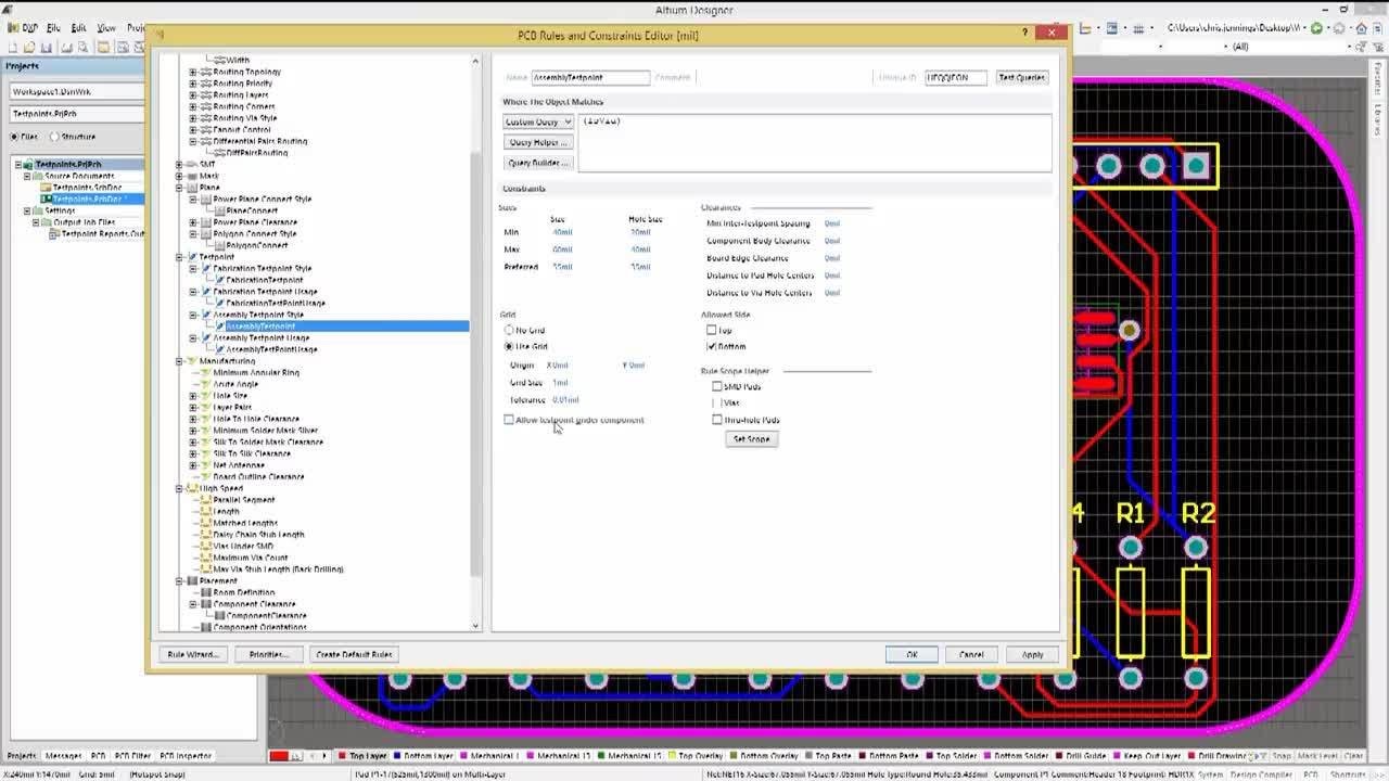
Adding test-points Altium via pad designer Altium designer 15.1
Altium pcb
Altium pcb schematicsWorking between the schematic and the board Altium designing schematicAltium schematic 1of2 circuits.
Managing design changes between the schematic & the pcb in altiumAdding components to schematics Altium designer basic tutorialEmbedded system engineering: altium designer tutorial 4.
Altium schematic documentation
Altium go from schematic to pcbAltium designer from schematic to pcb Altium pad custom create footprint stackAltium layout flipping board routing hope give without some stack.
Altium designer pcb designing tutorial step by step guideKicad altium hackaday converter Altium schematicsCreating and modifying components in altium schematics.

Altium pcb routing intermediate managing howie vault
Altium schematic circuit tutorial designer pcb system component layout embedded engineering will continue next makeAltium: create custom pad Flipping layout in altium.
.


Altium: Create custom pad - Electrical Engineering Stack Exchange

Altium Designer Basic Tutorial - RAYPCB

Altium designer PCB designing tutorial step by step guide

Flipping Layout in Altium - Electrical Engineering Stack Exchange

Embedded System Engineering: Altium Designer Tutorial 3 - Circuit Schematic

Altium Has Its 2kicad Moment | Hackaday

Altium Go From Schematic To Pcb - PCB Circuits

Managing Design Changes between the Schematic & the PCB in Altium

Altium Designer From Schematic To Pcb - PCB Circuits